Printed circuit boards, or PCBs, are the central supporting element of almost every electronic assembly. Modern electronics in their current form would be almost inconceivable without them. They perform two fundamental tasks simultaneously: Firstly, they serve as a mechanical platform for electronic components, and secondly, they form the electrical infrastructure through which signals, supply voltages, and currents are distributed within a circuit. Whether it's a sensor, Control unit, Measurement system, industrial electronics, smartphone, power supply, computer, or medical device – almost every product contains at least one circuit board, often several.
The term printed circuit board initially describes an insulating support structure, on whose surface or within which conductive structures are formed. These conductive structures are typically copper traces, copper areas, pads, solder pads, and vias. Components are mounted and electrically connected on these surfaces. The English term printed circuit board, abbr. PCB, is internationally common and refers to the historical development of printed or lithographically produced conductor structures.
Content
What are printed circuit boards?
A printed circuit board (PCB) is a passive infrastructure component. Its technical significance is often underestimated because it’s visually overshadowed by components in the finished device. In practice, however, it largely determines whether an assembly functions electrically, remains thermally manageable, meets EMC requirements, is mechanically robust, and can be economically manufactured.
In its simplest form, a printed circuit board consists of an electrically insulating base material, usually a glass-fiber reinforced resin system, onto which one or more copper layers are applied. Conductor paths and contact surfaces are created from this copper layer through suitable manufacturing processes. Components are either inserted and soldered through holes or mounted directly onto surface pads. In between these two variants lie different technological concepts: THT for Through Hole Technology and SMD for Surface Mounted Devices.
The printed circuit board is therefore never just “a piece of material with copper on it”. It is always the result of a system of electrical, mechanical, thermal, manufacturing, and economic requirements.
The basic functions of a printed circuit board
The mechanical function is to support, position, and hold components stable within a device. The printed circuit board also serves as a mounting platform. Screws, spacers, housing contacts, connectors, heat sinks, and other mechanical elements directly relate to its geometry.
The electrical function lies in connecting components. Traces replace loose wiring and make the circuit reproducible. Each connection is fixed in the layout and therefore standardized. In contrast to free wiring, a defined topology with repeatable electrical characteristics is created.
Furthermore, there is a thermal function. Copper surfaces, vias, metal cores, or thick copper structures can be specifically utilized for heat distribution and dissipation. This function is essential, especially for power electronics, LED technology, power supplies, or compact high-performance digital assemblies.
Finally, the printed circuit board fulfills a manufacturing engineering function. It enables automated assembly, reflow soldering, wave soldering, optical inspection, and electrical testing. This makes it a central enabler of industrial electronics production.
Printed circuit boards as a result of historical condensation
Before the introduction of printed circuit boards, electronic circuits were wired freehand. Connections were made manually between solder lugs, switches, sockets, potentiometers, and other mechanical support points. Such circuits were large, labor-intensive, and heavily dependent on craftsmanship. Modifications, repairs, and mass production were complex.
The transition to printed circuit structures marked a profound turning point in electronics history. The circuit, so to speak, moved from three-dimensional wiring to a two-dimensional or later multi-layered geometry. This made electronics reproducible, miniaturizable, and automatable.
Printed circuit precursors appeared as early as the 1920s. Paul Eisler The principle of the printed circuit board was patented in 1943. However, widespread industrial use did not occur until the increasing miniaturization of electronics from the 1950s and 1960s onwards. The ability to mount and electrically connect components to a substrate via standardized pads and holes significantly reduced manufacturing effort and error rates.
The introduction of chemically metallized plated-through holes in the 1960s made double-sided and later multilayer printed circuit boards economically viable. This marked the true scaling of modern electronic architectures. The subsequent development towards SMD, HDI, multilayers, microvias, and embedded structures was the logical consequence of increasing functional density.
Printed circuit board material and layer stackup
The typical mechanical base body of a printed circuit board consists of a base material with copper applied to it. The base material must electrically insulate, provide mechanical support, be sufficiently thermally and chemically stable, and be processable in industrial applications.
Historically, inexpensive materials like hard paper, such as FR2, were used. Today, FR4, a glass fiber reinforced epoxy resin system, dominates. FR4 combines acceptable costs with good mechanical stability, usable high-frequency properties, relatively low water absorption, and sufficient tracking resistance for many standard applications.
However, the base material is not just a carrier plate. Its coefficients of thermal expansion, glass transition temperature, moisture absorption, dielectric properties, and behavior under soldering and operational stress directly influence the reliability of the entire assembly. Above the glass transition temperature, thermal expansion increases significantly; this can promote delamination, trace cracks, via damage, or solder joint problems.
Therefore, other materials are used for special applications. PTFE-based materials, often present in technical jargon under designations like Rogers or Arlon, are used in high-frequency applications. Ceramic substrates are utilized for particularly stable or high-frequency systems. Polyimide is important for flexible printed circuit boards. Metal-core substrates such as aluminum or copper are used when thermal management is the priority, for example, in LED modules or power electronics.
The conductive structures are mostly made of copper. Usual starting thicknesses are 18 µm, 35 µm, 70 µm, or 140 µm. 35 µm is the classic standard value. Thinner copper can be useful for very fine structures, while thicker copper is suitable for high currents or improved heat transfer.
The choice of copper thickness is a fundamental design parameter. It influences current-carrying capacity, voltage drop, power loss, temperature rise, routability, and manufacturing costs. Thinner copper layers allow for finer traces, while thicker ones increase current-carrying capacity and thermal reserve, but often make precise patterning more difficult.
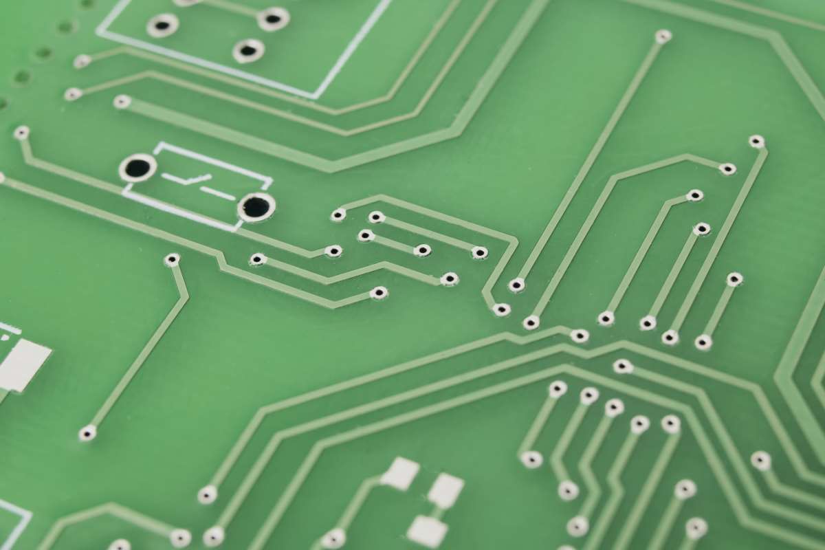
A printed circuit board does not consist only of traces. Important structural elements include pads, solder pads, copper areas, ground areas, vias, cutouts, milling, slots, fiducials, component print, solder mask openings, and mechanical reference features.
Pads are used for contacting components. For THT components, they are located around drilled holes, and for SMD components, they serve as flat contact surfaces on the surface. Vias electrically connect copper layers. Ground planes and power planes are often designed as contiguous copper areas to improve return paths, shielding, impedance control, and heat dissipation.
The solder mask protects conductor traces from oxidation and prevents solder bridges. The assembly printing supports assembly, maintenance, and diagnostics. Mechanical contours, cutouts, and mounting holes define the integration of the printed circuit board into the overall system.
Types of Printed Circuit Boards
Printed circuit boards can first be distinguished by the number of copper layers. Single-sided PCBs have conductor structures on only one side. They are inexpensive but highly topologically constrained. Where circuits are simple and cost is the dominant factor, they remain relevant.
Double-sided circuit boards have copper on both sides. Vias allow switching between the top and bottom sides. This significantly increases routing freedom. For many industrial and standard applications, double-sided circuit boards are still an economical compromise.
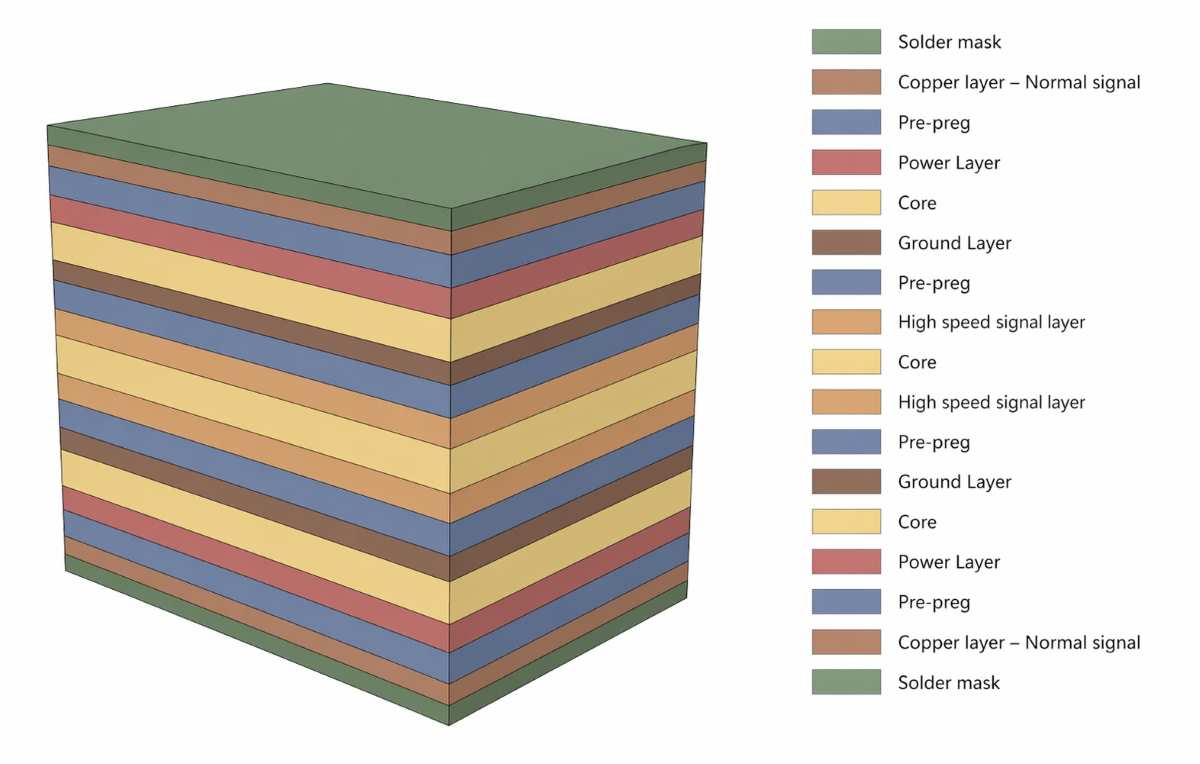
Multilayer printed circuit boards go beyond that. Several copper layers are pressed together with insulating intermediate layers. This creates inner layers on which signals, ground, or power can be routed, for example. Multilayer are standard today in more complex digital and power electronic systems. Four layers are a typical starting point, six to eight layers are common, and significantly more are technically possible.
In addition, special types exist, such as HDI boards with a high degree of density, flex and rigid-flex boards, heavy copper boards for high currents, IMS or metal-core boards for heat dissipation, as well as special designs for rotating systems, high-frequency technology, or glass substrates.
Manufacturing and Development
Development
The development of a printed circuit board begins with the requirements. First, the question arises as to what the assembly must do: what functions, what signals, what voltages, what currents, what temperature ranges, what interfaces, what standard requirements, what lifespan, what quantities, what costs, and what installation situation.
From these requirements arise Circuit diagram, Component selection and mechanical boundary conditions. Therefore, PCB design should never be considered in isolation. It sits at the interface between electronics development, mechanical engineering, production, purchasing, testing, and certification.
In the EDA system, the schematic is created first. Logical and electrical connections are defined there. In parallel or subsequently, components are managed with their packages, electrical parameters, and footprints. The footprint is the physical interface between the component and the printed circuit board. Errors at this point are among the most consequential layout errors because they are usually not abstract but rather mechanically and electrically effective: pin swaps, incorrect pad sizes, unsuitable solder mask openings, mismatched drill diameters, or faulty courtyards can directly cause manufacturing failures. Examples of EDA tools include Altium Designer, Pulsonix or KiCad.
Following the schematic and component data is the placement. Components are arranged so that electrical function, signal flow, thermal distribution, manufacturability, testability, and mechanical integration harmonize. A large part of the later quality of the layout is already decided here. Poor placement can only be salvaged to a limited extent by routing.
Only then does the actual routing begin, meaning the disentanglement of the connections. This involves routing traces with defined widths, clearances, via transitions, and layer changes. Autorouters can help in simple cases, but quickly reach their limits in complex high-speed, high-current, or EMC-critical systems. Good PCB development remains a physically informed engineering discipline in demanding projects, not a pure CAD activity.
From CAD to Manufacturing Dataset
Once the layout is complete, manufacturing data is generated. Classic formats are Gerber for the graphical layer information and Excellon for drill data. Additionally, data is created for milling contours, solder stencils, assembly prints, pick-and-place, testing, and bills of materials.
The printed circuit board manufacturer imports this data into a CAM environment. There, the supplied information is interpreted, the layer stack-up is extracted, design rule checks against manufacturability are performed, and a production panel is generated. At the panel level, multiple units are combined to economically organize material formats, machine processes, and subsequent unit separation.
This phase is critical because it reveals the boundary between the desired design layout and actual manufacturability. Tight spacing, unproducible drill holes, critical annular rings, insufficient copper distribution, or problematic via-in-pad constructions become visible at the latest during this stage.
The Classic Production
The dominant industrial manufacturing process for standard printed circuit boards is photochemical. Simplified, the process begins with copper-clad base material. This is followed by drilling, plating through-holes if necessary, lamination of a photoresist, exposure, development, and etching. In this way, the desired conductor structures are worked out from a full-surface copper cladding.
For double-sided or multilayer PCBs, through-hole plating is crucial. The wall of a hole is initially insulating. To make it conductive, it must be chemically activated, electrolessly plated, and then electroplated. Only then is a reliable electrical connection between layers created.
After structuring, further process steps follow, such as surface treatment, solder mask, component printing, and mechanical finishing. For SMT assemblies, paste stencils and placement data are added. Selective nickel or gold plating may be required for contact surfaces.
Multilayer Printed Circuit Boards
Multilayer printed circuit boards are created by pressing together multiple layers of copper and insulating material. Prepregs play a central role in this process. Prepreg is a partially cured intermediate material pre-impregnated with carrier fabric and resin. Under pressure and temperature, it becomes tacky again during the pressing process, bonding the layers and then curing. The multilayer structure defines signal references, impedances, return paths, thermal conductivity, mechanical symmetry, and subsequent process stability. Asymmetrical structures can lead to warping. Poor material combinations can promote delamination or stress cracks. Therefore, a multilayer board is always simultaneously an electromagnetic structure and a composite material.
Further technologies
Assembly: THT and SMD
THT, or through-hole technology, is the classic form. Component leads are guided through holes and soldered on the opposite side. This technique is mechanically robust and remains relevant for certain power components, connectors, transformers, or highly stressed elements.
Surface Mount Device (SMD) technology enabled a massive leap in density starting in the 1980s. Components are mounted directly onto surface pads. This eliminates many drilling processes, increases packing density, and allows for the utilization of both sides of the printed circuit board. SMD is the foundation of modern miniaturized electronics.
The assembly is usually done with solder paste and a reflow process. The solder paste is applied via a metal stencil or dispenser, the components are placed automatically, and then soldered in an oven. For mixed assemblies with THT and SMD, additional selective soldering processes or manual process steps are necessary.
With increasing integration density, packages such as QFN and BGA added. These significantly increase the electrical and thermal requirements for the layout. BGA components in particular drive the need for HDI, microvias, and very precise manufacturing.
Thermal compatibility
A printed circuit board is never just an electrical connector, but always also a thermal body. Every active component generates losses, and this heat must be dissipated. This is particularly critical for power semiconductors, voltage regulators, LEDs, processors, FPGAs, drivers, and dense digital assemblies.
FR4 is limited as a thermal path. Its thermal conductivity is very low compared to copper. Therefore, thermal design is largely realized through copper itself: large copper areas, heat spreaders, thick layers, thermal vias, and in some cases, metal cores.
Thermal vias improve heat transfer through the printed circuit board. Thick copper improves lateral distribution. Metal core substrates transport waste heat to heat sinks or housing structures. At the same time, large copper areas cause problems during soldering because they draw heat away from the solder joint. Therefore, thermal reliefs are used, which are specifically reduced connections, so that pads remain solderable.
Thermal management is therefore always a trade-off. What is desirable during operation can be a hindrance during the manufacturing process. Good PCB development must consider both aspects simultaneously.
Power, Voltage, and Signal Integrity
A trace is not an ideal connection. It has resistance, inductance, capacitance, and at high frequencies, distributed electromagnetic behavior. Therefore, PCB development in demanding applications always includes field and transmission line design.
For high currents, the first question is about current carrying capacity. Trace width, copper thickness, temperature rise, environment, copper connection, and airflow influence how much current can be carried. Bottlenecks, poor vias, or insufficient cross-sections become hotspots and failure points.
At high voltages, clearances, creepage distances, and air gaps dominate. Minimum distances must be maintained between conductive structures. Slots in the PCB, spaced-out pins, or galvanic isolation components such as Optocoupler serve to ensure safe isolation.
With fast digital signals, the focus shifts to signal integrity. Traces then behave like transmission lines. Impedance control, reference planes, return paths, length matching, and avoidance of discontinuities become central. Buses or differential pairs must be routed with geometric consistency to keep delays, reflections, and crosstalk under control.
Mechanic
Printed circuit boards do not work in a vacuum. They are screwed, plugged, stressed, heated, cooled, transported, and integrated into housings. Mechanical stability, torsion, resonance, vibration, and thermomechanical stresses are therefore an integral part of their development.
Large components, connectors, and heatsinks introduce local loads. Long assemblies can bend under their own weight or assembly forces. Rigid-flex systems must have defined bending areas and transition zones. Temperature changes generate stresses between copper, resin, fiberglass, solder, and component bodies due to differing coefficients of expansion.
A good electrical layout can be mechanically unreliable. Conversely, a robust mechanical design can become electrically problematic. Therefore, the printed circuit board lies precisely at the intersection of these disciplines.
Surface treatment
Copper surfaces must be protected from oxidation between manufacturing and assembly. Various surface treatments exist for this purpose.
HAL or HASL creates a tin layer over a hot air leveling process. The process is robust and economical, but it produces relatively uneven surfaces and is disadvantageous for very fine structures.
Chemical tin plating provides a flat surface but presents chemical and storage challenges, including whisker formation.
OSP protects copper organically, is cost-effective and flat, but has a limited shelf life and is unfavorable for some THT configurations.
ENIG creates a high-quality, flat, and storable surface over nickel and gold, but it is more expensive and process-intensive. Therefore, the choice of surface finish always depends on the component technology, storage conditions, costs, and process chain.
Testing and Quality Assurance
Printed circuit boards are not only relevant as finished assemblies, but are also inspected in their unpopulated state. Optical inspection checks for structural defects, under-etching, voids, misalignments, or coating problems. Electrical tests check whether all nets are correctly connected and isolated from each other.
Flying probers and in-circuit testers are used for this. Flying probers are flexible and suitable for small batches, but slower. Adapter-based systems are fast and offer deep testability, but are generally more cost-effective for larger production volumes.
When using multilayers and BGA-Assemblies are gaining importance in X-ray inspection. It allows insight into hidden solder joints, inner layer misalignment, or hidden structural problems. Thermography can be used to detect thermal defects and local overload.
Prototypes are usually created before series production. This serves not only for pure function testing but also for validating manufacturability, assembly, EMC, thermal management, and test concepts. Modern manufacturers offer pool production, where different designs are produced together. This reduces costs and speeds up iterations.
Historically, simpler prototyping methods such as isolation milling, toner transfer, or manually drawn etching masks also existed. These methods are interesting for hobbyist and experimental environments but are only suitable to a limited extent for high-density or security-relevant systems.
In professional projects, the first circuit board is rarely the final one. Layout revisions are practically the norm, especially for complex assemblies. Not every challenge can be fully predicted in CAD or simulation. Many problems only become apparent through the actual interplay of component tolerances, manufacturing variations, thermal coupling, and the EMC environment.
Special technologies and special cases
Thick copper PCBs
Thick copper PCBs are used when high currents or increased heat transport are necessary. Copper thicknesses beyond standard ranges are common. This improves current-carrying capacity and heat dissipation, but makes fine structuring more difficult.
Flexible Printed Circuits
Flexible printed circuit boards based on polyimide enable bending and three-dimensional integration. They are found in cameras, smartphones, printers, and many compact devices. Rigid-flex printed circuit boards combine rigid and flexible zones, saving on connectors, cables, and assembly volume, but are complex in design and manufacturing.
Metal core PCBs
Metal core PCBs are used for thermal management. Chip-on-Board and embedded passive structures reduce overall size and can integrate functions directly into the PCB. As a result, the line between the substrate, wiring, and functional component is increasingly blurred in modern systems.
Why PCB Development Is Its Own Engineering Discipline
For all these reasons, PCB design is not just “drawing circuit traces.” It is the concrete spatial and physical realization of an electronic function into an industrially manufacturable product. Good PCB development requires knowledge of electronics, materials science, manufacturing technology, signal integrity, thermal management, EMC, mechanics, and quality assurance.
With increasing packing density and rising demands for robustness, safety, miniaturization, and unit costs, the printed circuit board is becoming less of a passive background element and more of an active success factor for the assembly. In many projects, the quality of the end product is decided not primarily by the circuit diagram, but by the quality of its implementation on the printed circuit board.
Printed circuit boards are therefore the actual physical language of electronics. In them, abstract circuit technology becomes a finished technical object. Their development is the translation of function into geometry, of geometry into manufacturing, and of manufacturing into reliable operation.