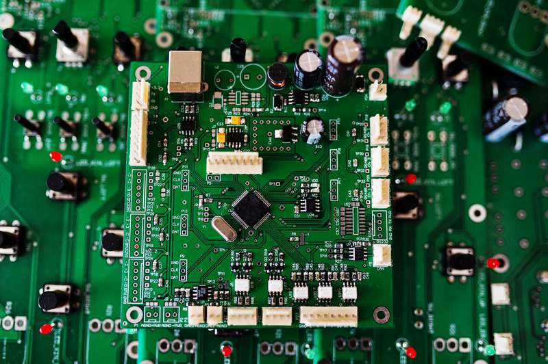
Layer„, also known as“PCB Layer,“ in German „Lage“ or „Schicht“ (meaning layer or sheet), describes the structural makeup of a printed circuit board. The goal of every Hardware Development This refers to the development of a compound made of multiple layers for PCB manufacturing. Modern PCBs consist not only of visible conductive traces on the top and bottom sides, but also of multiple superimposed copper and insulating layers. Together, these form the electrical and mechanical foundation of electronic systems.
Content
The layer stack-up influences almost all properties of a hardware platform. This includes routing capabilities, power supply, signal integrity, electromagnetic behavior, thermal properties, and mechanical stability. Especially in embedded systems, industrial electronics, communication hardware, or high-speed systems, selecting the correct stack-up is a central component of the hardware architecture.
A PCB essentially consists of conductive and non-conductive materials. The conductive layers are typically made of copper. Insulating materials such as FR4 or special high-speed laminates are located between these copper layers. The different layers are pressed together under pressure and temperature, forming a stable laminate.
PCB Layer
The PCB layers perform different functions. Some of the layers are used for signal routing. Digital and analog signals are transmitted between microcontrollers, processors, sensors, memory, or interface components via these layers.
In simple designs, signals are exclusively on the top and bottom layers of the printed circuit board. However, as complexity increases, these two layers are no longer sufficient. Additional internal layers enable a higher wiring density while simultaneously improving the electrical quality of the system.
In addition to signal layers, dedicated ground planes exist. These are among the most important layers in modern printed circuit boards. A ground plane provides a stable electrical reference potential and serves as a return path for electrical signals. Especially with fast digital signals, the return current flows directly below the trace along the reference plane. This creates small loop areas with lower electromagnetic radiation.
In addition to ground planes, power planes are often used. These distribute electrical voltages within the PCB. Complex systems often have several power planes for different voltages such as 5 volts, 3.3 volts, 1.8 volts, or various core voltages of modern processors and FPGAs.
Dielectrics and Insulation Layers
Between PCB layers are insulating materials, referred to as dielectrics. They define the mechanical stability and simultaneously influence the electrical properties of the printed circuit board.
Important parameters of these materials are the dielectric constant and the loss factor. These properties, together with trace width, copper thickness, and distance to the reference plane, determine the impedance of signals. High-speed interfaces such as USB, Ethernet, PCIe, or DDR memory require precisely defined impedances, which is why the construction of the dielectric layers must be precisely controlled.
FR4 is often used as the standard material. However, for particularly fast or high-frequency systems, special materials with better HF properties are used.
PCB Layer Stackup
The sequence of all copper and insulation layers is called the layer stack-up. The stack-up defines the complete structure of the PCB and is among the most important technical parameters of a printed circuit board design.
For example, a typical 4-layer stack consists of a top signal layer, a ground plane, a power plane, and a bottom signal layer. The internal reference planes create defined return current paths and stable electrical characteristics.
For more complex systems, 6-, 8-, or even more-layer stack-ups are used. Additional inner layers enable separate routing areas, better shielding, and higher wiring densities.
The stack-up is not just a mechanical description of the PCB, but an essential part of the electrical system architecture.
Typical Layer Counts of Modern PCBs
Simple consumer electronics or cost-sensitive embedded systems often use 1- or 2-layer PCBs. These are suitable for low wiring densities and slow signals. However, limits are quickly reached with EMC requirements or more complex routing tasks.
4-layer PCBs are considered the standard today for many microcontrollers and embedded systems. Dedicated ground and power planes significantly improve both the signal integrity and electromagnetic behavior of the printed circuit board.
6-layer PCBs are often used in industrial controls, communication systems, or automotive electronics. The additional inner layers create more routing capacity and allow for better separation of sensitive signals.
8-layer PCBs and larger stack-ups are primarily used in high-speed systems. These include motherboards, FPGA platforms, MPSoCs, DDR memory interfaces, or high-data-rate communication hardware.
In servers, network technology, or military electronics, significantly more than 10 or 12 copper layers can also be used.
Meaning for Signal Integrity and EMC
As data rates increase, PCB layers become increasingly critical. High-speed signals require defined return paths and controlled impedances. Errors in layer construction can quickly lead to reflections, crosstalk, EMI problems, or timing errors.
The close coupling between the signal and reference planes is particularly important. Fast signals should be routed as directly as possible over a ground plane. This keeps the return current path short and electromagnetic radiation low.
Connected ground planes also act as shielding between adjacent signals and reduce crosstalk within the PCB. For interfaces such as PCIe, USB 3.x, Ethernet, or DDR memory, a cleanly defined stack-up is therefore one of the fundamental development requirements.
Symmetric design and mechanical stability
Multilayer PCBs are constructed as symmetrically as possible. An asymmetrical structure can lead to mechanical stresses within the laminate. This can cause the circuit board to deform or warp during the soldering process or due to temperature changes.
For this reason, multilayer PCBs mostly have an even number of layers, such as 4, 6, or 8. Odd stack-ups are significantly less favorable from a manufacturing perspective and are rarely used in practice.
The mechanical symmetry also improves the long-term stability of the circuit board under thermal stress.
Relationship between layers and vias
Once multiple copper layers exist, through-holes are needed. These so-called vias electrically connect different layers.
Classic through-hole vias go through the entire printed circuit board. In addition, there are blind vias and buried vias, which only connect specific layers. Modern HDI designs often use microvias to enable very high wiring densities.
The number and type of vias used depend directly on the layer structure and the complexity of the system.
Layer in modern embedded systems
As electronic systems become increasingly integrated, the number of required PCB layers also increases. Modern embedded systems often contain powerful processors, high-speed memory interfaces, radio modules, Ethernet interfaces, and complex power supplies within a limited space.
This results in high demands on routing, EMC, thermal behavior, and power distribution. Multilayer PCBs enable the necessary structuring of these systems and form the basis of modern electronic platforms.
Specifically, FPGA systems, MPSoC platforms, or safety-critical electronics require clearly defined layer structures with controlled electrical properties.
Conclusion
Layers form the structural and electrical foundation of every PCB. They determine how signals are routed, how power is distributed, and how stable an electronic system operates under real-world conditions.
While simple embedded systems often get by with two or four layers, modern high-speed systems require complex stack-ups with numerous reference and power planes.
The layer structure is therefore not purely a manufacturing issue, but a central component of hardware architecture, signal integrity, and electromagnetic compatibility of electronic systems.