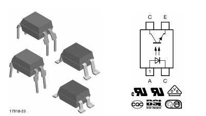
An optocoupler transmits an electrical signal via an optical path. On the input side, there is usually an infrared LED, and on the output side, a light-sensitive semiconductor element. There is no conductive connection between the two sides. This allows signals to be transmitted between circuit parts with different ground potentials without direct current flowing across the isolation point.
Content
A typical example of this construction type is the Vishay VO615A. It combines a GaAs infrared LED with a silicon phototransistor in a 4-pin package. The component thus belongs to the group of phototransistor optocouplers. This version is suitable for discrete switching signals, level shifting, feedback signals, and simple isolated interfaces. For the Hardware Development An optocoupler is therefore a welcome component for implementing electrically safe signal paths.
Classification: What is an optocoupler?
An optocoupler is an isolation component for signals. It galvanically separates two electrical areas and transmits the information state optically. The input side is operated like an LED. The output side of the phototransistor type behaves similarly to a light-controlled NPN transistor.
In an electronic system, an optocoupler separates, for example:
- Microcontroller logic for mains voltage ranges,
- Control boards for power electronics,
- various mass potentials in industrial plants,
- Primary and secondary side of a switched-mode power supply,
- Sources of interference for sensitive signal acquisition.
The term „optocoupler“ does not describe a single circuit architecture. There are phototransistor optocouplers, logic optocouplers, optotriacs, PhotoMOS relays, and linear optocouplers. The VO615A represents the classic phototransistor variant: LED in, optical coupling across an isolation gap, transistor current at the output.
How an optocoupler works
In a phototransistor optocoupler, current flows through an infrared LED on the input side. The LED emits light onto the phototransistor. This generates a collector current as soon as enough light hits its base region. The output current depends on the LED current, the coupling within the housing, the transistor's operating point, the temperature, and component tolerances.
The most important parameter is the Current Transfer Ratio, or CTR. It describes the ratio of output collector current to input LED current:
CTR = Click-Through Rate IC = Impressions Clicked IF = Impressions Found
A CTR of 100 % means that, at an LED current of 5 mA, a collector current of approximately 5 mA can flow under the specified test conditions. In data sheets, the CTR is not specified as a fixed value, but rather as a range. For the VO615A, there are batches with different CTR ranges. This variation is critical for design purposes because the circuit must function even with the smallest permissible CTR value.
The output of a phototransistor optocoupler is not an actively driven logic output. It requires external circuitry, usually a pull-up resistor to the output supply voltage. When the LED lights up, the phototransistor conducts and pulls the collector node towards the emitter. With a typical pull-up circuit, this results in an inverted signal: LED on means low output, LED off means high output.
The VO615A is specified for a high isolation test voltage. The datasheet mentions 5300 VRMS as the test voltage between the input and output sides. This value describes a defined test of the isolation system. For circuit design, creepage distances, air gaps, pollution degree, overvoltage category, and the required working or rated voltage according to the respective equipment standard are also important.
Typical architecture in the system
The input side of an optocoupler usually has a logic source, a transistor driver, or a voltage evaluator. A series resistor or a constant current source is connected in series with the LED. The series resistor determines the LED current:
RIN = (VIN – VF) / IF
Here, VF is the forward voltage of the LED. It changes with current and temperature. The LED can also only withstand limited reverse voltage. If AC voltage or negative voltage can occur at the input, an antiparallel diode or other protective circuit is required.
The optical isolation path lies between the input and output sides. It prevents a conductive current path between the two reference potentials. However, a small capacitive coupling remains. For the VO615A, the datasheet indicates a low coupling capacitance between input and output. This capacitance can cause common-mode currents across the barrier during rapid voltage jumps.
On the output side, the phototransistor works with its own reference ground and its own power supply. A simple circuit consists of:
- Collector to pull-up resistor,
- Pull-up resistor to power supply,
- Emitter to ground,
- Collector nodes as a logic signal.
Alternatively, the phototransistor can drive a subsequent transistor stage, a comparator, a digital input, or a driver. For larger load currents, the optocoupler should not be directly considered a power switch. The phototransistor in the VO615A is designed for small signal currents; loads such as relays, valves, or MOSFET gates require a downstream driver stage.
Signals and Communication in Optocouplers
A 4-pin phototransistor optocoupler typically has the following connections:
- Input LED anode,
- Cathode of the input LED,
- Emitter output transistors,
- Collector of the output transistor.
The signal direction runs from the LED to the phototransistor side. Reverse transmission is not possible with this structure. For bidirectional interfaces, two optocouplers, special digital isolators, or isolated transceivers are used.
The input level is defined by the LED current, not directly by a logic voltage. A 3.3V or 5V microcontroller pin can drive an optocoupler if the pin can supply or sink the required current and the series resistor is chosen accordingly. For higher input voltages, such as 12V or 24V in industrial environments, the series resistor is sized larger. The power dissipation in the resistor must then be checked.
No fixed CMOS or TTL levels are generated at the output by the component itself. The level is determined by the external supply, the pull-up resistor, and the phototransistor current. For a safe low level, the following must apply:
The current flowing through the pull-up must be less than the collector current that the optocoupler can supply at minimum CTR.
Additionally, the saturation voltage of the phototransistor must match the input thresholds of the subsequent logic. The datasheet for the VO615A specifies a low collector-emitter saturation voltage for the phototransistor under defined conditions. In the circuit, this value depends on the LED current and the load current.
The timing of phototransistor optocouplers is limited by several effects. The LED requires a short time to turn on and off. The phototransistor has capacitance and charge storage effects. When operated deep in saturation, its turn-off time increases. Additionally, the pull-up resistor forms an RC element with the collector capacitance and the input capacitance of the following circuit.
The VO615A has switching times in the microsecond range, depending on load resistance and operating conditions. This class is often sufficient for slow status signals, power supply feedback, or digital control signals. For fast data transmission, isolated UART links with high baud rates, SPI, or precise PWM acquisition, logic optocouplers or digital isolators are better suited.
Operating modes and operating states
A phototransistor optocoupler has no internal registers, no enable pin, no reset state, and no sleep mode. The operating states result from LED current and the output circuit.
When in the off state, no current flows through the LED. The phototransistor is largely blocked. The pull-up resistor then sets the collector node to high at the output, provided the output supply is active. A dark current from the phototransistor remains. This is small but must be considered for high-ohm pull-ups and high temperatures.
In the ON state, LED current flows. The phototransistor becomes conductive. With a pull-up circuit, the collector voltage drops. Depending on the load current, the transistor operates in the linear region or in saturation. For digital signals, it is often operated in saturation because this results in a low logic level. The disadvantage is a longer turn-off time.
An intermediate range occurs at low LED currents, aged LEDs, high temperatures, or low CTR. In this range, the output level can become undefined if the switching threshold of the subsequent circuit is not reached with sufficient margin. Therefore, for digital inputs, a Schmitt trigger is recommended, or dimensioning with sufficient current spacing between the ON and OFF states.
A standby mode is only available system-side. If the input power is switched off, the LED remains off. If the output power is switched off, the output signal is invalid, even if the LED is lit. Since the two sides are galvanically isolated, each side can be supplied or switched off independently. Protective circuits must prevent unwanted feedback through external signal paths.
Power supply
An optocoupler such as the VO615A does not have a supply pin. The input side is powered by the LED current. The output side is connected to the supply there via the external pull-up or load circuit.
- On the entry page, the following points must be checked:
- maximum continuous LED current,
- permissible impulse currents and pulse duration,
- LED forward voltage at temperature,
- reverse standoff voltage,
- Power loss in the series resistor.
LED current selection is a compromise between available output current, power dissipation, aging, and switching speed. Higher LED current increases photocurrent but burdens the driver more and increases power dissipation. Lower LED current reduces power requirements but requires a CTR design with more headroom.
On the output side, supply voltage and pull-up resistor determine the collector current:
IC ≈ VOUT / RPULLUP
For a 5V logic with a 10kΩ pull-up, approximately 0.5mA flows in the low state. For the same low level with a 1kΩ pull-up, approximately 5mA would be required. The smaller pull-up speeds up the rising edge but requires more output current and thus more LED current or a higher CTR.
The VO615A phototransistor is specified for a collector-emitter voltage up to the range of typical signal and control levels; the datasheet names 80 V as the maximum collector-emitter voltage. This limit must not be exceeded, even when the phototransistor is switched off. Inductive loads or long cables may require additional overvoltage protection measures.
Power sequencing with simple optocouplers is less determined by the component itself and more by the connected circuit parts. If the output supply is active earlier than the input side, the output remains in its idle state via the pull-up. If the input side is active and the output side is missing, no valid logic level can be generated. Subsequent logic should tolerate such states or they should be intercepted via defined pull-ups, pull-downs, and reset circuits.
Blocking capacitors do not belong directly on the optocoupler as there is no supply pin. They belong on the driver and evaluation circuits on both sides of the isolation. Short current loops at the LED driver and a clean supply to the output logic reduce false triggering from voltage drops and interference pulses.
Application framework for optocouplers
Phototransistor optocouplers are used for slow to medium digital signals when galvanic isolation is required. Typical applications include isolated status signals, error outputs, input channels in controllers, power supply feedback, relay or driver controls across an isolation barrier, and decoupling different ground potentials.
In switched-mode power supplies, an optocoupler frequently transmits a feedback signal from the secondary side to the primary control. In this process, the LED current is usually controlled via a reference regulator or error amplifier. CTR variations and aging are generally compensated for by the control loop. For precise linear measurement transmission, a simple phototransistor optocoupler is only suitable to a limited extent because CTR and temperature behavior do not guarantee accurate current transmission.
In industrial inputs, optocouplers can transfer 24V signals to the logic level of a control board. The input resistor must then be chosen such that sufficient LED current flows at the minimum input voltage, and the LED and resistor are not overloaded at the maximum input voltage. For AC voltage inputs or inputs with polarity protection, additional diodes, rectifiers, or anti-parallel LEDs are required.
Limits arise from switching speed, CTR tolerance, LED aging, isolation requirements, and common-mode interference. For high data rates, components with a logic output and specified propagation delay are more suitable. For mains voltage switching tasks with triacs, optotriacs are used. For galvanically isolated solid-state relays, PhotoMOS optocouplers are used. The phototransistor type remains useful for simple switching signals if its variations are taken into account during dimensioning.
Layout and Routing Guidelines for Optocouplers
The layout must maintain the galvanic isolation of the optocoupler. Traces on the input side and output side must not shorten the isolation distance with copper areas, test points, components, or contamination paths. Creepage and clearance distances on the PCB must comply with the required operating voltage and equipment standard. The housing insulation of the optocoupler does not compensate for unsuitable PCB layout.
There should be no copper surface connecting both sides underneath the optocoupler. Likewise, separated ground planes must not be bridged by accidental copper remnants, shielding areas, or solder mask markings with conductive residues. For higher insulation requirements, slots are often used in the PCB to increase the creepage distance. Whether this is necessary depends on the voltage, standard, and degree of pollution.
The input loop consisting of the driver, series resistor, and LED should be kept short. This reduces coupling into the LED line and limits radiated interference with fast edges. For long input lines, series resistors, RC filters, or protective diodes against transient voltages may be necessary.
On the output side, the pull-up resistor affects the slew rate. A very high pull-up saves current but slows down the rising edge and increases sensitivity to leakage currents. A low pull-up speeds up the level change but requires more phototransistor current. The line from the collector to the subsequent logic input should not be unnecessarily long, as additional capacitance will increase switching time.
The thermal load in phototransistor optocouplers is mainly determined by LED current, output current, and ambient temperature. Input and output power losses add up within the package. The datasheet specifies limit values for the LED, transistor, and total power dissipation. With dense component placement or increased ambient temperature, the LED current should not be at the upper limit without a reserve.
During EMC tests, rapid common-mode voltage changes can generate interference currents through the internal coupling capacitance of the optocoupler. Short reference paths, defined pull-ups or pull-downs, and suitable filters on long lines reduce spurious triggering. For environments with very fast common-mode transients, an optocoupler with specified common-mode transient immunity or a digital isolator should be considered.
Zurück zum Glossar