BGA stands for Ball Grid Array and refers to a design for integrated circuits (ICs) in which the electrical connections are arranged as a matrix of small solder balls on the underside of the component. In contrast to classic packages such as QFP or SOIC, where the pins are routed out of the package on the sides, the contacts in a BGA are located entirely under the component. Consequently, the individual solder points are no longer visible after assembly on the circuit board.
Content
The solder balls form a regular grid through which the component is connected to the printed circuit board. This grid can have different pitches depending on the component, often in the range of approximately 0.8 mm down to below 0.4 mm for highly integrated components. BGAs are primarily used for complex semiconductors, such as microprocessors, FPGAs, memory components, or high-performance System-on-Chip components.
Use of BGA components
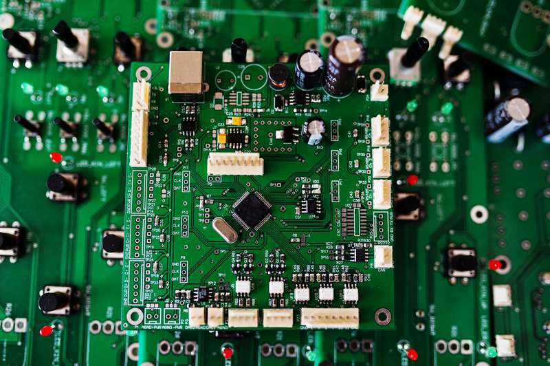
BGA Package Assembly
A BGA essentially consists of several structural elements:
- the actual silicon chip (die) inside the housing
- to the substrate, which serves as a carrier for the internal wiring
- a matrix of solder balls on the underside
- internal bond connections between chip and substrate
The solder balls perform two functions simultaneously: they establish the electrical connection to the printed circuit board and ensure a mechanical attachment of the component.

How does BGA assembly work?
The assembly of a BGA is generally fully automated. First, solder paste is applied to the corresponding pads of the printed circuit board. Then, a pick-and-place machine precisely places the component onto the printed circuit board.
In the subsequent reflow soldering process, the assembly is heated in a controlled manner. The solder balls melt and connect with the pads on the printed circuit board. Due to the surface tension of the solder, the component often self-aligns precisely during melting.
Since the solder joints are located under the component, they cannot be visually inspected. Therefore, the quality of the solder connections is usually checked using X-ray inspection (AXI).
Advantages of BGA packages
BGA packages have become established in many areas of electronics due to the technical advantages they offer.
A significant advantage is the high connection density. Due to the grid arrangement of the contacts, considerably more pins can be realized in the same area than with laterally led connections.
Furthermore, BGAs often offer better electrical performance. The connections are very short, which reduces parasitic inductances. This is particularly relevant for high-frequency signals and fast digital interfaces.
The thermal properties are also often more favorable. The large contact surface under the component allows for more effective heat dissipation through the printed circuit board.

Challenges in PCB Design
The high connection density of BGA components places special demands on PCB layout. The signals must be routed out of the tight grid of the solder balls. This process is called fanout.
Typical layout techniques include:
- Routing between pads with larger pitch distances
- Use of Microvias for Small Pitch Dimensions
- Via-in-Pad Technology in High-Density Designs
- Using HDI PCBs (High Density Interconnect)
Especially with modern BGAs with very small pitch values, multilayer PCBs and advanced routing strategies are necessary.
Debugging challenges
Besides the advantages, BGAs also bring some practical challenges. Since the solder joints are located under the component, they are not directly accessible. This makes both troubleshooting and repairs difficult.
Typical challenges include:
- Limited signal-level debugging capabilities
- Difficult rework or repair of faulty solder joints
- necessary X-ray inspection for quality control
- additional need for test points for important signals
In particular, when developing embedded systems, a larger number of test pads or debug interfaces are often provided to enable later analysis.
Meaning for embedded systems
BGA packages are a central component of modern embedded hardware today. Many high-performance components—such as microprocessors, FPGAs, or memory—are only available in BGA package designs. Developers must therefore plan their PCB layout as well as their test and debug strategies accordingly.
The use of BGA components enables compact and powerful electronic systems, but at the same time places high demands on PCB design, manufacturing processes, and quality assurance.