EMC is rarely the primary topic at the beginning of a development project. EMC problems are insidious and only arise long after the initial development iterations. In the early stages, functionality, component selection, and PCB layout are the main focus. However, if EMC requirements are not systematically considered from the outset, the costs for troubleshooting will significantly increase later in the project.
In the concept and design phase, EMC aspects can usually be considered with little effort: through appropriate topologies, suitable components, sensible partitioning of the circuit, and basic layout rules. Adjustments in this phase cause hardly any additional costs, as they are part of the normal development work. Important in the Hardware Development is therefore above all the knowledge of the most important and pressing problems of EMC.
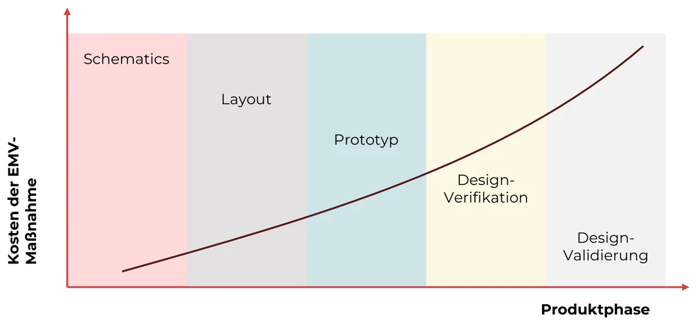
After the initial hardware build, the conditions change drastically. If EMC problems only appear after the PCB assembly or during preliminary tests and certification tests, corrections become significantly more complex. Layout changes, additional filters, shielding measures, or even a PCB redesign incur direct costs for development, new prototypes, and re-testing. Added to this are indirect costs due to delays and blocked resources.
It becomes particularly critical when EMC problems are only detected in late phases such as design verification, validation, or just before product release. At this stage, EMC deficiencies often lead to multiple hardware revision iterations, delays in market launch, or, in extreme cases, project cancellations. The costs do not increase linearly, but exponentially with each later phase.
The most common EMC problems in PCB design
EMV problems arise from specific physical effects on the printed circuit board and connected lines. The causes are rapid changes in current and voltage, parasitic inductances and capacitances, as well as unfavorable return paths. Certain interference sources repeatedly occur and can be observed independently of the application or device category.
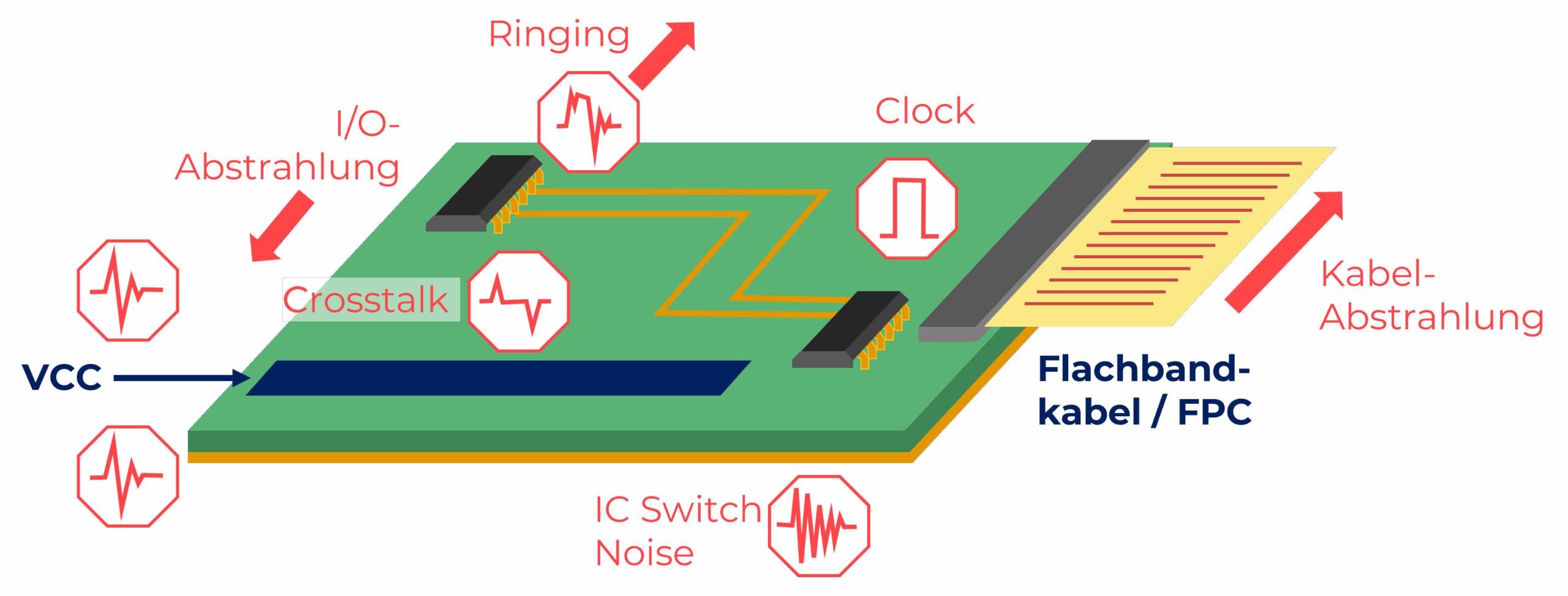
IC Switching Noise
When switching internal logic structures, very rapid current changes occur. These high di/dt values generate broadband interference that is directly fed into supply and ground connections. IC switching noise is often the origin of many other EMC effects, as it can propagate throughout the entire printed circuit board.
Transients in the supply voltage
Due to parasitic inductances in traces, vias, and bond connections, the supply voltage reacts sensitively to rapid load changes. The result is temporary voltage drops or overshoots on Vcc. These Vcc transients influence the switching behavior of the ICs and increase the high-frequency component of the emissions.
Disturbances and Influences of Clock Signals
Clock signals have steep edges and therefore a broad spectrum of harmonics. Even at comparatively low fundamental frequencies, clock signal lines can cause significant electromagnetic interference. Long lines, missing reference planes, or missing damping significantly amplify this effect.
Ringing and Overshoot Due to Impedance Mismatches
Ringing occurs when the line impedance does not match the driver or receiver. Reflections cause overshoot and undershoot on the signal edges, which significantly increases the high-frequency content of the signal. These additional frequency components directly and negatively impact EMC behavior.
Crosstalk between traces
In dense routing, signals capacitively and inductively couple into adjacent traces. Crosstalk manifests as interference pulses on otherwise quiet signals. This is particularly critical for parallel routing of fast signals without sufficient spacing or missing reference planes. There are now analysis tools for the effects of crosstalk, for example in the form of Signal integrity testing.
Printed circuit board radiation
Die Leiterplatte kann als Antenne wirken. Große Stromschleifen, unterbrochene Masseflächen oder resonante Kupferstrukturen führen dazu, dass hochfrequente Störungen direkt vom der Platine abgestrahlt werden und deren Leistung beeinträchtigen. PCB radiate. PCB radiation is often a consequence of unfavorable return current paths and lack of area continuity.
Radiation at inputs and outputs
I/O pins represent a direct coupling between internal switching operations and the outside world. Rapid signal changes at these pins lead to local radiation. Without damping or filtering, I/O radiation can quickly develop into a dominant EMC problem.
Cables as transmitting antennas
Connected cables act as very efficient antennas. Common-mode noise that enters the cable from the PCB is radiated with high efficacy. Cable radiation is one of the most common reasons for failing EMC tests, even when the PCB alone appears inconspicuous.
Conclusion
Most EMC problems can be traced back to a few clearly identifiable sources of interference. The key factor is not a single effect, but rather the interaction between IC switching noise, Vcc transients, and disturbed signals, as well as the resulting radiation via the PCB, I/Os, and cables. Understanding these relationships allows one to identify EMC problems early on and take targeted measures to prevent them.