A CAN transceiver connects a CAN controller to the differential CAN bus line. The CAN controller generates and processes the logical bit sequences of the CAN protocol. The transceiver translates these logic signals into the physical levels on CANH and CANL and converts the bus signals back into a digital receive signal.
Content
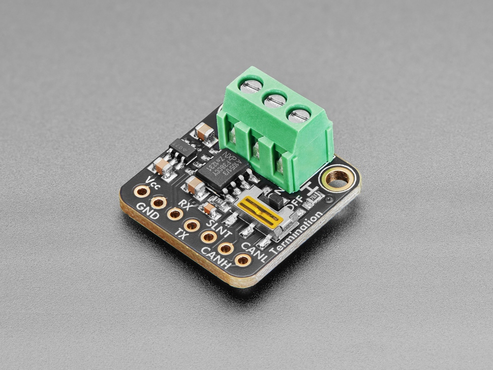
A building block like the NXP TJA1043 shows the typical functional scope of a high-speed CAN transceiver for automotive and industrial environments: 5V bus driver, separate logic supply for microcontroller levels, wake-up functions, low-power modes, inhibit output for supplying a control unit, and protection functions against fault conditions. Simpler variants like Infineon's TLE9250LE or microchips MCP2562 implement the same physical CAN basic mechanism, but differ in operating modes, control pins, logic supply, and system management.
What is a CAN transceiver?
A CAN transceiver is the physical interface of a CAN node. It sits between the digital CAN controller and the twisted-pair bus. On the controller side, it works with logic signals like TXD and RXD. On the bus side, it drives or receives the differential lines CANH and CANL.
The CAN controller can be in Microcontroller integrated or present as a separate controller IC. It processes frames, identifiers, arbitration, bit stuffing, CRC, and error states of the protocol. The CAN transceiver, on the other hand, handles the electrical implementation:
- Sending a dominant or recessive bus state
- Differential bus level reception
- Level adjustment between logic side and bus side
- Limiting error effects to the bus
- Behavior on undervoltage, overtemperature, or permanently dominant TXD
- Switching to power-saving states
- Detection of wake-up events, by type
In High-Speed CAN according to ISO 11898-2, the bus is typically at a common level around the midpoint of the transceiver supply in the recessive state. In the dominant state, CANH is raised and CANL is lowered. The receiver evaluates the differential voltage between CANH and CANL. This makes the signal less susceptible to common-mode noise than a purely ground-referenced single-wire transmission.
How a CAN Transceiver Works
The digital input TXD controls the transmitter section. In High-Speed CAN, a dominant state usually corresponds to a low level on TXD. The transceiver then drives CANH towards a higher voltage and CANL towards a lower voltage. In a recessive state, the bus is not actively forced into differential dominance. The bus lines then remain close together, and the differential level remains small.
The receiver compares CANH and CANL. If the differential voltage is large enough, the receiver recognizes a dominant bus state and outputs this to the CAN controller via RXD. In the case of a recessive bus state, RXD is correspondingly in the recessive logic state.
This behavior forms the basis of CAN arbitration. Multiple nodes can transmit simultaneously. A dominant state overwrites a recessive state on the bus. The CAN controller detects via RXD whether the read bus state matches the transmitted TXD state. The protocol decision lies with the controller; the transceiver provides the electrical prerequisite.
A transceiver like the TJA1043 supplements this basic path with monitoring and protection logic. This typically includes:
- TXD-Dominant-Time-out, so that a blocked controller does not hold the bus permanently dominant
- Undervoltage detection on supply connections
- Thermal shutdown or transmitter limiting
- Defined initial states in case of missing supply
- Wake-up detection via bus or separate wake input
- Status output via dedicated pins, depending on the IC
The exact implementation is manufacturer-specific. The TJA1043 has a pronounced system management section with a VBAT connection, INH output, and local and bus-side wake-up mechanisms. A compact component like the TLE9250LE focuses more on the physical high-speed CAN interface. The MCP2562 is an alternative example with separate VIO logic supply and standby control, but without the same system basis functionality as a TJA1043.
Typical architecture in the system
A CAN node typically consists of a microcontroller, CAN controller, CAN transceiver, power supply circuit, protection circuit, and bus connection. In many microcontrollers, the CAN controller is already integrated. In that case, only TXD and RXD run between the microcontroller and the transceiver.
A typical signal chain looks like this:
Microcontroller with CAN controller → TXD/RXD → CAN transceiver → CANH/CANL → Connector → twisted pair bus line
On the supply level, a 5V rail is often added for the transceiver. If the microcontroller operates at 3.3V or a lower logic voltage, a VIO connection separates the digital level side from the 5V bus driver side. The TJA1043 uses such a logic supply. The MCP2562 also provides a VIO variant, allowing RXD and TXD to be adapted to the controller's I/O voltage.
By Control units With a low-power requirement, the transceiver can influence parts of the supply. The TJA1043 has an INH output for this purpose. This can activate or deactivate an external voltage regulator. In sleep mode, a battery supply path is maintained for wake-up functions, while other circuit parts can be switched off.
On the bus side, CANH and CANL are on a twisted pair of wires. The bus is terminated at both ends, typically with 120 Ω. Individual nodes along the line do not have their own full termination unless they are at a bus end. In split termination, the termination is divided into two resistors, and the midpoint is connected to ground via a capacitor. Some transceivers, including the TJA1043, provide a SPLIT pin that sets the midpoint to a defined level.
Signals and Communication on the CAN Transceiver
The most important signals of a high-speed CAN transceiver are TXD, RXD, CANH, and CANL. Depending on the chip, there are also control, status, and power supply connections.
TXD is the digital transmission input. It comes from the CAN controller. A dominant TXD state leads to the dominant bus state as long as the transceiver is enabled for transmission and no protection function intervenes.
RXD is the digital reception output. It reports the detected bus state to the controller. RXD is also required during arbitration because the controller compares the actual read bus state with the sent bit.
CANH and CANL form the differential bus pair. In the dominant state, CANH rises above the recessive common mode, while CANL is lowered. In the recessive state, both lines are close to each other. The receiver evaluates the differential voltage, not the absolute level of a single line.
EN, STB, STBY, or comparable pins control the operating state. With the TJA1043, the modes are selected via EN and STB_N. With the MCP2562, the standby state is controlled via STBY. With the TLE9250LE, the specific control depends on the package and variant assignment; compact high-speed CAN transceivers often use an Enable or Normal Mode pin instead of multiple system management lines.
WAKE is an input on transceivers with local wake-up functionality for an external event, such as a button, a sensor signal, or a terminal in the Control unit. The TJA1043 can also be woken up from a low-power state.
INH is an output for the power supply circuit. It can enable or disable an external regulator. This feature is more commonly found in transceivers with advanced low-power management.
ERR_N or comparable status pins report internal states. With the TJA1043, such a pin can signal wake-up or error states, among other things. The meaning must match the selected operating mode in the firmware.
SPLIT provides a reference point for split termination with suitable transceivers. This allows the common-mode level of the recessive bus to be stabilized. Whether this pin is used depends on the EMC concept, termination type, and system topology.
Timing parameters include transmission delay, reception delay, loop delay, and edge behavior, among others. For classic High-Speed CAN with up to 1 Mbit/s, these values must be designed for the bit time. For CAN FD data phases with higher bit rates, transceivers, controllers, line length, and sampling points must be considered together. The TLE9250LE is specified by Infineon for CAN FD applications with higher data rates, while older or simpler transceiver families are partly designed for classic CAN.
Operating modes
A CAN transceiver has at least a normal mode and usually a low-power mode. Components with system management offer additional modes.
In normal operation, the transmitter and receiver are active. TXD controls the bus, and RXD reports the bus status. This mode is used for regular CAN communication.
In standby mode, the transmission path is switched off or blocked. The receiver only operates as far as necessary for bus monitoring or wake-up detection. Power consumption decreases compared to normal operation. With the MCP2562, this state is accessible via STBY. RXD can continue to indicate a wake-up or bus state depending on the component.
In sleep mode, power consumption is further reduced. In the TJA1043, this state can be coupled with the INH output. This allows an external regulator to be switched off, while the transceiver can detect wake-up events via a battery supply path.
A listen-only or silent state, if available, allows receiving without actively transmitting on the bus. This is used for diagnostics, bus monitoring, or states where a node should not exert bus dominance. The exact naming and availability depend on the IC.
Reset and undervoltage conditions occur when a supply drops below a specified threshold. The transceiver must then prevent undefined logic states from disturbing the bus. Datasheets describe for these cases whether RXD is high-impedance, dominant, recessive, or status-dependent, and whether the transmitter is switched off.
Wake-up can occur via the bus or a local input. With bus wake-up, the transceiver detects defined activity on CANH/CANL. With local wake-up, a level change on a pin like WAKE is evaluated. After waking up, the firmware must read status flags or evaluate pins so that the source of the event is handled correctly.
Power supply
High-speed CAN transceivers typically operate with a 5 V supply on the bus side. In the examples mentioned, the transceiver supply is around 5 V; the exact limit values are given in the respective data sheets. This supply powers the analog receiver, the bus driver, and parts of the protection logic.
A separate logic supply, VIO, allows for adaptation to the microcontroller's I/O voltage. This applies to TXD, RXD, and control pins. With a 3.3V microcontroller, VIO prevents a 5V RXD level from being directly fed to the controller input. The TJA1043 and MCP2562 use this principle. For transceivers without VIO, the logic levels must match the controller side.
A VBAT connection, as found on the TJA1043, supplies low-power and wake-up functions from the battery or an always-on rail. This allows the transceiver to trigger a wake-up even when the regular 5V rail is turned off. Battery power is not intended for the CAN bus driver during normal operation; the transmitter still requires the regular transceiver supply.
Power sequencing particularly affects systems where Microcontroller, VIO, VCC, and VBAT are supplied at different times. The transceiver must not drive the bus in an undefined state when the logic supply is missing. Likewise, an active RXD output must not feed back into an unpowered controller I/O via protection diodes. Datasheets indicate which pins are tolerant to specific supply failures and which states are internally forced.
Bypass capacitors should be placed close to the supply pins. The 5V pin of the transceiver requires a short connection to ground because the bus driver causes current spikes when switching. VIO and VBAT also receive local bypassing according to datasheet and system requirements. For vehicle supplies, protection measures against load dumps, reverse polarity, transients, and ESD are added. The CAN transceiver does not replace this external protection and supply design.
Application framework
CAN transceivers are used in control units that communicate via a CAN bus. Typical areas include vehicle control units, trailer and commercial vehicle systems, battery management, chargers, industrial drives, machine controls, sensor-actuator nodes, and diagnostic devices.
The TJA1043 is suitable for systems requiring wake-up from sleep states and a controllable power supply. In such architectures, the INH output can influence the controller's regulator. The combination of bus wake-up, local wake-up, and status signals requires appropriate firmware logic, as the microcontroller must put the transceiver into the desired state after power-up.
A TLE9250LE shows a different design: The focus is on a compact high-speed CAN interface, which can also be specified for CAN FD data phases. Such components are used when bus communication is the priority and an extensive wake/inhibit system is not needed in the transceiver.
The MCP2562 is an alternative example of a transceiver with separate VIO logic supply and standby function. It suits systems where the microcontroller operates with lower I/O voltage, while the CAN bus driver is supplied from 5V. The operational control is simpler than a system-base transceiver with VBAT, INH and multiple wake sources.
Limits are imposed by bus length, bit rate, topology, termination, interference, ground offset, and permissible common-mode ranges. A CAN transceiver does not provide galvanic isolation. If significant potential differences can occur between nodes, a digital isolator or an isolated CAN transceiver is also required. Protocol capability is also not generated in the transceiver. Filters, identifier processing, error counters, and frame handling remain the responsibility of the CAN controller.
Layout and Routing Guidelines for CAN Transceivers
The CAN transceiver should be placed close to the bus connector. This keeps CANH and CANL short on the PCB. Protection components such as TVS diodes are usually located close to the connector so that ESD and transient currents are not routed through the entire PCB.
CANH and CANL are routed as a differential pair. The traces should be of similar length and maintain a consistent spacing. Stubs should be kept short, especially at higher bit rates or for CAN FD data phases. The PCB impedance must match the bus environment; the cable bus itself is typically considered to have approximately 120 Ω differential impedance.
Termination belongs on both ends of the bus. In split termination, two resistors with a center tap are used. This center tap can be bypassed to ground via a capacitor. If a SPLIT pin is present, it can supply this point with a defined DC level. The benefit depends on the EMC concept.
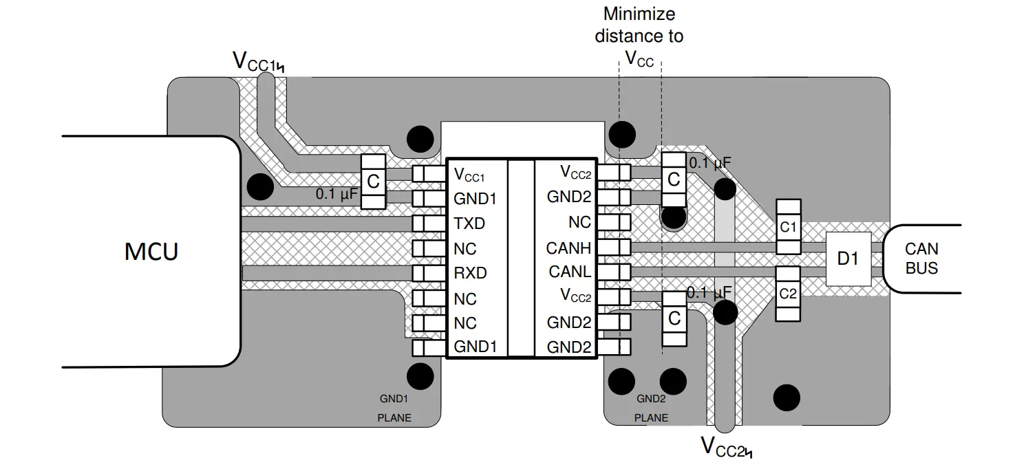
The mass feed should consider the return path of the supply and the protection path of the bus circuitry. The transceiver requires a low-impedance ground connection. ESD currents from the connector should be routed via a short path to the designated protective or chassis ground without passing through sensitive logic areas.
The TXD, RXD, and mode lines are routed short and without unnecessary coupling to switching power signals. Upon microcontroller reset, the TXD and mode pins must have defined levels. An unintentional dominant TXD state can block the bus until the transceiver's timeout function intervenes. Pull-ups or pull-downs should be designed according to the datasheet and system startup behavior.
The supply pins receive local decoupling capacitors. VCC, VIO, and optionally VBAT should be considered separately because they supply different functions within the IC. For packages with an exposed pad, the thermal and electrical connection must be made according to the manufacturer's specifications. The bus driver can generate power dissipation at high bus loads and elevated ambient temperatures, even if the average current during normal operation is usually low.
Zurück zum Glossar