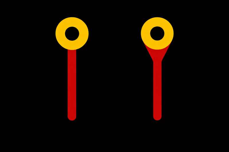
What are teardrops?
Teardrops are teardrop-shaped copper extensions at the connection between a trace and a pad or Via on a printed circuit board. They are used in PCB layout to improve the mechanical and electrical robustness of these transitions. Teardrops increase the reliability of the printed circuit board, especially with fine structures or tight manufacturing tolerances.
Background and Motivation
During the manufacturing of printed circuit boards, holes for vias or THT pads are created after the copper structure has been etched. During this process, minimal drill misalignments can occur, where the drill hole deviates slightly from its ideal position.
Without additional copper area, such an offset can lead to:
- the annular ring is partially or completely removed
- the trace has only minimal contact with the via or pad
- in the worst case, the connection is interrupted
Teardrops therefore widen the transition area between the trace and the pad, creating additional copper reserve.
Operating principle
A teardrop enlarges the copper area at the transition from a trace to a pad or via in a teardrop shape. This creates a larger overlap between the trace and the plated through-hole.
The advantages are:
- Higher manufacturing tolerance for bore offset
- lower risk of open connections
- better mechanical stability under thermal loads
This can be crucial, especially with very narrow traces or small vias.
Areas of application
Teardrops are typically used for:
- HDI PCBs with very small structures
- High-density BGA fan-out layouts
- Traces with very small widths
- Designs with high mechanical or thermal loads
Many modern EDA tools like Altium Designer or KiCad can automatically generate teardrops.
Significance in modern PCB design
In many standard designs, teardrops are optional. However, in high-density or safety-critical applications, they are considered good layout practice. They increase robustness against manufacturing tolerances and help ensure electrically stable connections in the long term.