A TVS diode is a semiconductor device for limiting short overvoltage pulses. TVS stands for Transient Voltage Suppressor. The component is connected in parallel to a power rail, a signal line, or an interface and remains high-impedance during normal operation. If the voltage exceeds a defined range, the diode breaks down and conducts the surge current to the return line, ground, or chassis structure. Within the scope of Hardware Development Does the TVS diode stand for standard components for voltage supply and protection? EMVrelevant signals.
Content
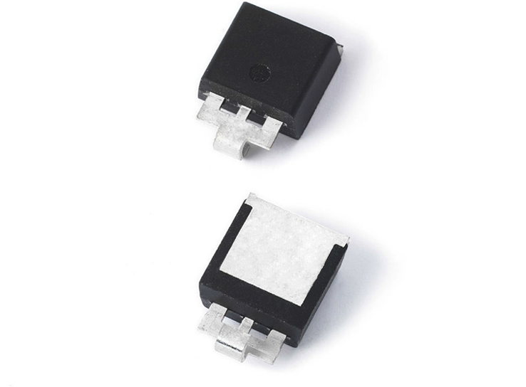
The Littelfuse SM8 series is a prime example of a powerful building block on a power rail. According to the datasheet, it belongs to the SM8S series with 6600 W peak pulse power with a 10/1000 µs pulse waveform. The SM8S36A variant is unidirectional, has a reverse stand-off voltage of 36 V, and clamps surges above its avalanche region. Such components are often used where automotive, industrial, or power supplies need protection against surge pulses, inductive switching spikes, or similar transient events.
Classification: What is a TVS diode?
A TVS diode is a discrete protective component with a defined nonlinear characteristic curve. Its function is voltage limitation during short transient events.
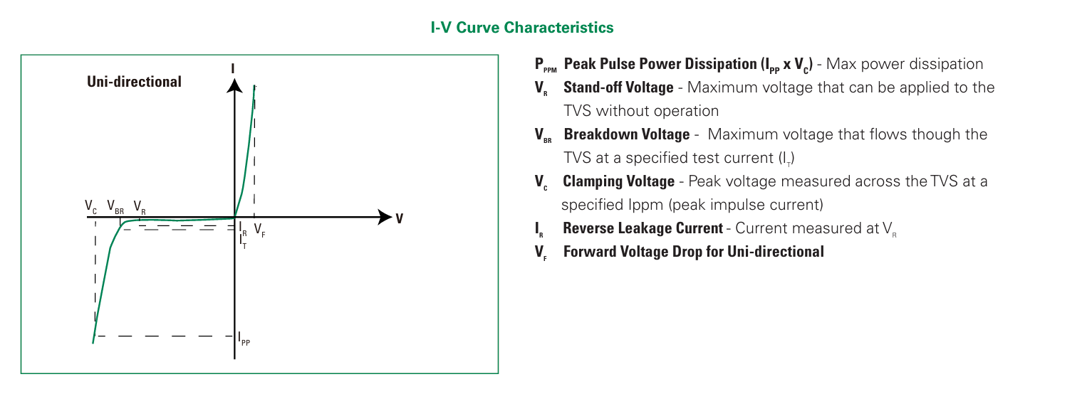
In its normal operating state, the supply voltage is below the so-called reverse stand-off voltage. In this range, only a small leakage current flows. In the event of an overvoltage, the current through the TVS diode increases sharply. The voltage across the protected circuit is thereby limited to a clamping voltage. This clamping voltage is above the normal operating voltage but must remain below the voltage rating of the subsequent circuit.
TVS diodes with high surge power are often used for supply rails. The SM8S36A is a good reference component for this: it is specified for a 36 V reverse stand-off voltage, has a breakdown voltage of 40.0 V to 44.2 V according to the datasheet, and achieves a maximum clamping voltage of 58.1 V at a specified peak pulse current. These values show the typical gradation of a TVS diode: normal operating voltage, breakdown range, and clamping voltage under surge load.
How it works
The basic principle is based on the avalanche breakdown of a p-n junction. Below the specified reverse voltage, the diode blocks. If the reverse voltage becomes so high that the breakdown region is reached, the current rises very steeply. The diode briefly absorbs energy and converts it into heat.
In reverse bias, a unidirectional diode exhibits the avalanche characteristic. In forward bias, the component behaves similarly to a normal diode. This allows negative overvoltage to be dissipated to ground via the forward characteristic. In contrast, a bidirectional TVS diode has a similar breakdown characteristic in both polarities and is often used for AC signals, differential lines, or interfaces with alternating polarity.
The term „clamping“ does not describe an ideal voltage limiter. The clamping voltage depends on the pulse current, pulse shape, temperature, and parasitic inductances in the current path. The datasheet of the SM8S36A specifies the maximum clamping voltage at a defined peak pulse current. With very fast current rises, additional voltage can arise across trace and connection inductances. The voltage actually present at the load is therefore higher than what the pure semiconductor characteristic would suggest.
A TVS diode is not designed for continuous voltage regulation. This distinguishes it from a Zener diode, which functions as a reference or stabilizing component in certain circuits. TVS diodes are designed for short pulses with defined energy and pulse shape. If the permissible energy is exceeded or if there is a continuous overvoltage, the component can be thermally overloaded.
Typical architecture in the system
A TVS diode is usually located close to where interference can enter the device. For a power rail, this is often the input behind the connector. This is followed by a fuse, reverse polarity protection, filter, etc., depending on the system., Washington D.C.DC-DC converter, LDOs, load switches, or the actual load.
A simplified structure for a protected supply looks like this:
Connector → Fuse or Current Limiter → TVS Diode to Ground or Chassis → Input Filter → Converter or Load
The exact order depends on the protection concept. If the TVS diode is placed directly behind the connector, it can absorb a large part of the surge current before it enters the printed circuit board. An upstream fuse or current limiting can prevent the TVS diode from being permanently overloaded in case of prolonged faults.
In vehicle electrical systems and with long cables, overvoltages frequently occur due to inductive loads, switching operations, load shedding, or external interference. Therefore, a TVS diode on a supply close to 24V or 36V must be selected such that normal operating peaks do not trigger it. At the same time, the clamping voltage must not drive the downstream electronics beyond their permissible limits.
For signal lines, the focus is different. Capacitance, leakage current, and signal distortion need to be considered more closely. A high-power TVS like the SM8S36A is typically suited for power rails, not for high-speed data lines. For USB, Ethernet, CAN, LIN, or RF-adjacent signals, TVS arrays with low capacitance and appropriate line geometry are used.
Signals and Communication for a TVS Diode
A TVS diode has no communication interface and no control pins. The relevant terminals are anode and cathode. For unidirectional components, the polarity is fixed. The cathode is usually connected to the rail to be protected during positive supply, and the anode to ground or return. The marking on the housing indicates the cathode side.
The electrical „signals“ of a TVS diode are the voltage and current states at its terminals:
Below the reverse stand-off voltage, the TVS diode remains high impedance. For the SM8S36A, this limit is 36 V. The leakage current in this range is low and is specified in the datasheet as Reverse Leakage Current.
Between standoff voltage and breakdown voltage, the component approaches the breakdown region. The breakdown voltage is specified at a defined test current. For the SM8S36A, according to the datasheet, it lies between 40.0 V and 44.2 V.
During a voltage surge, a high pulse current flows. The voltage across the component rises to the clamping voltage. For the SM8S36A, a maximum clamping voltage of 58.1 V is specified at the specified peak pulse current.
The timing is not comparable to digital setup or hold times. The semiconductor structure reacts very quickly to an overvoltage. However, in the real system, package inductance, trace length, ground routing, and the rise time of the disturbance pulse limit the actual protection effect. For steep pulses, every additional nanohenry in the discharge path generates an additional voltage according to V = L · di/dt.
For interfaces, this means: a TVS diode does not communicate with a controller. However, it affects signal quality through its parasitic capacitance, leakage current, and placement in the signal path. For supply rails, the capacitance is usually less critical than for high-speed data lines.
Operating modes of a TVS diode
A TVS diode has no operating modes like sleep, standby, reset, or enable. Its state results from the applied voltage and the available energy of the surge event.
In blocking mode, the voltage is below the reverse stand-off voltage. The component has no significant impact on the circuit. Only the specified leakage current flows.
In the transition region, the current increases with increasing voltage. This region should not be reached permanently during normal operation if power loss and heating are not factored in.
In avalanche operation, the TVS diode conducts the transient current. The energy of the pulse heats the pn junction. The peak pulse power rating is valid only for the pulse shape specified in the datasheet and the thermal boundary conditions defined there.
In the case of a negative voltage across a unidirectional TVS diode, the device conducts in the forward direction. This characteristic can be useful for negative transients but must be considered for reverse polarity or AC applications. Prolonged reverse polarity of a supply rail can cause high current if no additional current limiting is present.
After a permissible impulse, the TVS diode returns to reverse blocking mode. In case of overload, it can become permanently low-impedance or, in rarer cases, fail as high-impedance. The specific failure behavior depends on impulse energy, current source, thermal coupling, and package. Therefore, protection concepts with fuses or current limiting also consider the failure case of the protection component.
Power supply and dimensioning
A TVS diode does not require its own power rail. It is connected to the line to be protected and remains passive as long as the voltage is within the intended range.
The selection begins with the maximum continuous operating voltage of the line. The reverse stand-off voltage of the TVS diode must be above the highest normal voltage. This includes tolerances of the power supply, charging voltages, ripple, temperature drift, and short-term permissible operating peaks. If this margin is chosen too small, the TVS diode may increase leakage current or be thermally stressed during normal operation.
The breakdown voltage must be such that the component only triggers during actual overvoltage events. For the SM8S36A, the specified breakdown range starts above 40 V. Therefore, the component is not suitable for a 36 V rail that is operated continuously close to 40 V. It is more suitable for systems where 36 V is a sensible maximum continuous protection limit and subsequent components can tolerate a clamping voltage within the datasheet values.
The clamping voltage must be compared with the absolute maximum ratings of the protected circuit. A DC/DC converter, a load switch, or a MOSFET downstream of the TVS diode must withstand the remaining voltage, including parasitic surge components. The clamping voltage from the datasheet is tied to a defined pulse shape. Other pulse shapes can result in different current and temperature profiles.
The peak pulse power of the SM8S36A is specified as 6600 W at 10/1000 µs. This rating should not be interpreted as continuous power. For repeated pulses, higher ambient temperatures, or poor thermal coupling, the permissible power dissipation decreases. Datasheets contain derating curves for this, for example, for peak pulse power versus temperature or pulse duration.
Blocking capacitors do not replace a TVS diode. Capacitors reduce local voltage drops and filter high-frequency components. A TVS diode, on the other hand, limits high transient voltages by shunting current. In many input circuits, TVS diodes, capacitors, ferrites, chokes, or resistors are combined. The sequence and sizing determine which current path is created during a pulse.
TVS Diode Application Framework
TVS diodes are used on lines where short voltage surges can occur. Typical areas include power supply inputs, automotive onboard networks, industrial electronics, relay and solenoid valve environments, long cables, sensor supplies, and interfaces with external access.
A powerful single TVS such as the SM8S36A is suitable for supply rails with significant surge currents. The package and electrical design are designed for high pulse energy. For data lines, such a component would generally be unsuitable due to capacitance, package size, and routing. Smaller TVS diodes or multi-channel TVS arrays are used there.
The system boundaries result from several points:
The TVS diode can only absorb as much energy as its thermal and electrical design allows. A permanent surge fault must be managed via fuse, switch, current limiting, or power supply shutdown.
The clamping voltage is higher than the operating voltage. Subsequent components require sufficient voltage resistance.
The discharge path to ground or chassis determines part of the protective effect. A TVS diode in the wrong place may become conductive but still allow the surge current to flow through sensitive circuit parts.
The polarity must match the application. Unidirectional TVS diodes are suitable for DC rails with defined polarity. Bidirectional variants are better suited for lines where both polarities can occur during normal operation or in fault conditions.
The standard or test pulse shape must be suitable for the application. Specifications such as 10/1000 µs, 8/20 µs, ESD according to IEC 61000-4-2, or load dump profiles are not interchangeable. A component with high performance for one pulse shape does not automatically meet every other surge requirement.
Surface-level requirements for layout and routing
Placement determines the protective effect more strongly than the pure datasheet value of the clamping voltage would suggest. A TVS diode should be placed close to the connector or the point of disturbance entry. The current path from the terminal, via the TVS diode, to the return path must be short and wide.
In supply rails, the TVS diode is routed in parallel between the line and ground or chassis. The connection to the ground plane should be low-inductance. Multiple vias can distribute the current if the discharge occurs onto an inner or rear copper plane. Long, narrow traces increase the additional inductive voltage during fast current rises.
The protected circuit should be located after the tap of the TVS diode. The surge current must not first flow through the trace to the load and then to the TVS diode. Otherwise, a voltage drop will occur along the trace, which will degrade the protection effect at the load.
With high pulse powers, the thermal connection to the housing must be suitable. Large copper areas help to dissipate the heat generated during a pulse. However, the thermal mass of the PCB does not replace the pulse specification of the component. Repeated pulses and high ambient temperatures must be checked against the derating information.
The mass concept depends on the system. In devices with chassis grounding, the return path can be directly to the chassis if the interference current is not supposed to flow through the signal ground. In purely potential-free electronics, the return current is usually routed through the local ground. Hybrid forms require a defined connection between protective earth, signal ground, and the housing to prevent unwanted current loops from forming.
For high-speed interfaces, the TVS diode should be integrated in such a way that the line impedance is disturbed as little as possible. For a high-power TVS on a power rail, on the other hand, low-inductive current discharge is paramount. The component should not be connected to the supply via a long stub, as this stub generates additional voltage during the pulse.
Zurück zum Glossar