Content
What is a Via
One Via is a conductive connection between different layers of a multilayer printed circuit board. It is realized by a drilled hole, the inner wall of which is metallized, thus creating an electrical connection between the copper layers. Vias are a central element of modern PCB layouts, as they enable the three-dimensional wiring of complex circuits.
Function of Vias
In multilayer printed circuit boards, signals not only run on one level but often have to switch between different layers. This is precisely where vias come into play. They enable:
- the exchange of signals between different PCB layers
- the connection of signal layers with power or ground planes
- The implementation of complex routing structures in high component density
Without vias, modern high-density layouts with microcontrollers or FPGAs in BGA form would be practically impossible to implement.
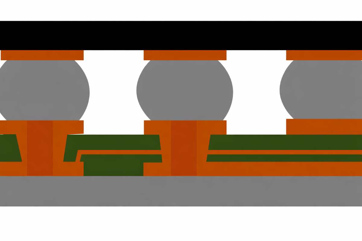
Building a via
A typical viaduct consists of several structural elements:
- Drilling: the mechanically drilled hole in the printed circuit board
- Metallization: a copper layer on the inner wall of the bore, which establishes the electrical connection
- Annular Ring: the copper ring around the hole on each layer
- Pad: the connection area of the via on the respective copper layer
The size of a via is usually determined by Drill diameter and pad diameter defined.
Types of Vias
In modern printed circuit boards, different via types are used, depending on the layer stackup and the required packing density.
Through ViasThese through-holes run through the entire printed circuit board and connect all layers. They are the standard in many designs and relatively easy to manufacture.
Blind ViasBlind vias connect an outer layer to one or more inner layers without penetrating the entire printed circuit board. They are used when routing area on the outer layers is limited.
Buried ViasBuried vias are located entirely within the printed circuit board and connect only inner layers. They are not visible from the outside and are typically used in highly complex multilayer designs.
Meaning in the layout
The placement and dimensioning of vias have a significant impact on:
- Signal integrity
- EMV behavior
- Manufacturability of the printed circuit board
- Routing density
Via transitions must be carefully planned, especially for high-speed signals or differential pairs, as they can cause impedance changes and reflections.
Vias in High-Density Designs
The introduction of Via-in-Pad technology is primarily driven by the increasing miniaturization of modern SMD components and the ever-denser arrangement of BGA packages (Ball Grid Arraydriven. With small ball pitches, there is often not enough space between the pads to route traces in the classic way.
In the Via-in-Pad process, the via is placed directly in the component pad. For this process to work reliably, the vias must be filled and then capped in a special manufacturing process (Filled & Capped Vias). It is crucial that no residues of process chemicals or voids remain in the via, as these can lead to soldering problems later on.
This setup allows traces to better integrate into other Layer to be routed. Particularly with components using BGA technology, this allows for additional routing channels between the pads, enabling significantly more complex and compact PCB layouts to be realized.
Dimensions and Requirements of the EMS
Printed circuit board manufacturers and EMS providers, such as. EuroCircuits typically define clear specifications within their Design Rules and manufacturing specifications. These guidelines set, for example, minimum and maximum values for drill diameters, pad diameters, annular ring, aspect ratio, or copper thicknesses, and ensure that the layout can be reliably manufactured with the respective manufacturing processes. Furthermore, they often contain specific requirements for special processes such as filling, via-in-pad, or different IPC-4761 via protection types, as these require additional process steps in production. It is therefore important for developers to consider the respective manufacturer guidelines as early as during PCB layout to avoid manufacturing problems, rework, or design iterations.
Conclusion
Vias are a fundamental element in printed circuit board design. They not only electrically connect different layers but also significantly determine how efficiently and reliably a layout can be implemented. In complex designs with many signals and high component density, they are indispensable.