
Military-grade PCBs are characterized by high climatic demands. Above all, however, they must work reliably for decades – often without the possibility of maintenance. Hardware Development from MIL Electronics are therefore subject to tight constraints early in the process.
In this article, we shed light on the technical standards and best practices that shape PCB design for military applications. From fundamental norms to material selection and specific design rules, we show what truly matters when developing electronics for the defense industry. They apply in addition to the requirements for Export control and the export of armaments as well as requirements regulatory in nature the NATO arms industry in general.
Content
Criteria from MIL-PRF-31032 for MIL Electronics
MIL-PRF-31032 is the central performance specification for rigid military PCBs and largely governs production and processing requirements. This standard not only establishes general performance requirements but also regulates which materials may be used, how manufacturing processes must be carried out, and which quality assurance measures are mandatory. In contrast to commercial standards, which allow for certain tolerances and deviations, MIL-PRF-31032 pursues a zero-defect philosophy. Among other things, clear requirements must be set for board and processing geometries, such as platings, drills, and annular rings. MIL-PRF-31032 is supplemented by MIL-PRF-50884 for specific manufacturing aspects and MIL-PRF-55110 for additional quality requirements. Together, these specifications form a comprehensive set of rules that cover every aspect of PCB design and manufacturing.
MIL-PRF-31032 specifies aspects such as ionic purity, adhesion strength, tensile strength, and resistance to moisture and thermal stress. Furthermore, it stipulates that materials, plating, and processing must be reproducible, durable, and suitable for use under demanding environmental conditions. Therefore, this standard is less of a design guideline and primarily targets manufacturing and validation processes. Engineering companies consider via dimensions, stackups, and trace spacing to each other and to outer dimensions within the scope of the standard.
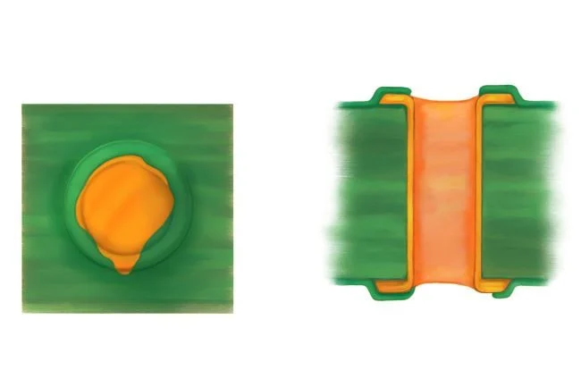
Plated-through hole accept-reject criteria. The test specimen has soldered successfully if solder has risen in all plated-through holes. The solder shall have fully wetted the walls of the plated-through hole. There shall be no exposed base metal or any non-wetting on any plated-through hole.
PRF-31032 for coated throughhole contacts
IPC-A-600 Class 3
IPC-A-600 is the globally recognized standard for the evaluation of the quality of electronic assemblies. It is absolutely essential for MIL electronics. It describes objective acceptance criteria for solder joints, mechanical attachments, surface finishes, component placement, and other features relevant to the reliability of electronic products.
The standard defines three classes that have different requirements for functional safety and operating environment:
- Class 1 – General Electronics
Products with limited lifespan and reliability requirements. - Class 2 – Controlgear with higher requirements
Devices that require stable operation over a longer period, e.g., industrial controls, communication devices. - Class 3 – Highly Reliable Electronics
Applications with critical requirements where failures are not tolerable, e.g., aerospace, medical technology, defense.
While MIL-standards primarily apply to U.S. military projects, IPC standards have become internationally established as a reference. For military applications, only IPC Class 3 is relevant.
A whole series of standards revolve around IPC-A-600, which set acceptance criteria for the finished assembled board as well as the PCB design. Meeting these standards is usually a joint task of designers, manufacturers, assemblers, and marketers.
For example, it is worth taking a look at the IPC-A-610 standard. IPC-A-610 defines acceptance criteria for electronic assemblies without specifying manufacturing processes or design rules itself. Each characteristic is classified into „target,“ „acceptable,“ „defect,“ and „process indicator,“ supplemented by rules for combined, unspecified, and special conditions.
This can be illustrated using round or embossed terminals: IPC-A-610 specifies a minimum solder joint height at the heel (F) for these terminals, which depends on the product class. For Class 1, the solder joint must reach at least the center of the outer terminal bend; for Class 2, at least the solder joint gap thickness G + 50 % of the terminal thickness T; and for Class 3, the solder joint gap thickness G + 100 % of the terminal thickness T. This breaks down the classification system into a concrete, measurable geometry that can serve as a reference for manufacturing, inspection, and rework.
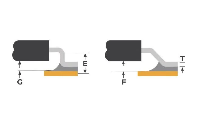
Ferse (F) must at least cross the midpoint of the outer connection bend → otherwise error. Class 1: Clearly visible wetting required
- Class 2: Minimum height F ≥ G + 50 % T
- Class 3: Minimum height F ≥ G + 100% TFalling below the respective minimum height → Class 2 or 3 error
Example IPC-A-610 Requirement for MIL Electronics
IPC Requirements for Layout and Schematics
For the development of MIL electronics, a variety of IPC standards exist. Not every standard is relevant for every design, but some documents form the core of what designers and manufacturers need on a daily basis.
Many of these standards are relatively specific and therefore extensive. For PCB designers, this means: the most important specifications should be directly embedded in the design rules, so that layout, manufacturing, and subsequent quality control are based on a consistent set of rules.
Among the frequently used and relevant IPC standards are:
- IPC-A-600TheAcceptance criteria, including classification into IPC Class 1, 2, and 3
- IPC-2221:Generic design and performance requirements for printed circuit boards
- IPC-4101:Material specifications for laminate and prepreg types, as well as stackup definitions
- IPC-2152: Current carrying capacity of conductor tracks
- IPC-4761:Categorization and Design Guidelines for Via Coverings and Via Protections
- IPC-6012Manufacturing and Quality Requirements for Rigid Printed Circuit Boards
- IPC-7351:Footprint and Land Pattern Design for SMD Components
- IPC-1752ASpecifications for material declaration and data exchange on ingredients
- IPC-6012E Requirements for Restriction and Mechanical Stability
- IPC-2581 Manufacturer-independent, data-consistent exchange format for manufacturing data that transports all manufacturing information in a structured model.
Typical Practices for MIL Electronics and IPC-Class 3 Designs
Class-3 products require increased mechanical stability, defined load capacity, and precise manufacturing. These include, in particular: teardrops at transitions between conductor tracks and ViaPad to avoid mechanical breakouts. Requirements for restrings according to IPC-6012E to stabilize the via structure against thermal and mechanical stress. Controlled impedance and signal integrity, especially for high-speed or RF circuits through defined trace widths, spacing, and stackup tuning. Thermal management, e.g., through thermally optimized layer structures, heat spreaders, via arrays, or thermal relief pads. These measures are typical for highly reliable assemblies and are clearly aimed at applications where electrical and mechanical stability are paramount – such as in aerospace, defense, industrial automation, or demanding sensor and control devices.
Stack-up symmetry
A completely asymmetric Stack-up is the enemy of every high-quality PCB. It leads to warpage, affects mechanical stability, and can make impedance uncontrollable. For Class 3 PCBs, a symmetrical construction is generally desirable. Symmetry refers to both layer thicknesses and copper weights. If a signal layer with 1 oz copper is on the top side, a signal layer with 1 oz copper should also be in the corresponding position on the bottom side. This balance ensures uniform impedance and minimizes crosstalk.
Power and ground planes should be placed directly next to each other. This arrangement creates a large-area capacitor that effectively suppresses high-frequency interference and minimizes electromagnetic interference (EMI).
Signal layers are preferably placed next to ground planes. This creates shorter return current paths and tighter coupling, which improves signal integrity and reduces emissions. In a typical 8-layer structure, this could look like this:
- Signal (Top)
- Ground
- Signal
- Power
- Ground
- Signal
- Ground
- Signal (Bottom)
A graphic representation as follows:

Teardrops
Teardrops are teardrop-shaped copper reinforcements at the transition point between a trace and a pad or via. In military electronics, they are used to increase the mechanical robustness of such transitions and to better compensate for manufacturing tolerances. Teardrops are particularly relevant in the area of fanouts, i.e., when routing signals out of fine component connections – such as with.
By increasing the copper area at the transition, teardrops stabilize these critical areas in the layout. They reduce the risk of traces detaching from the via due to drilling tolerances, vibration, or thermal cycling. At the same time, they distribute mechanical stresses more evenly within the copper. Teardrops reduce mechanical stress on via holes, thereby lowering the risk of microcracks or broken connections in high-stress electronic systems.

Requirements for Annular Rings
In military electronics systems, printed circuit boards have significantly stricter requirements for the annular ring than in many commercial applications. The annular ring refers to the ring-shaped copper area around a drilled hole or via. This area ensures that a reliable electrical connection between the pad and the drilled hole is maintained despite drilling tolerances, layer misalignment, or manufacturing variations. In MIL environments—such as in aviation, vehicle, or defense systems—printed circuit boards are exposed to significant mechanical and thermal stresses. For this reason, larger minimum widths of the annular ring are required to prevent failures due to breakouts, incomplete through-hole plating, or mechanical stresses. A generously dimensioned annular ring is an important robustness feature, especially for through-hole components, connectors, and mechanically stressed assemblies.

Connector Specifications
Another typical practice in the IPC Class 3 environment is the targeted use of U.S. Military Connector Specifications (MIL-DTL) - depending on whether interfaces are routed externally into a harsh operating environment or operate exclusively within protected systems. For robust outdoor applications, rugged circular connectors such as the MIL-DTL-38999 family are primarily used. These connectors are designed for extreme mechanical loads, humidity, vibration, shock, dust, and wide temperature ranges and are typically used for external connections in military environments, such as soldier systems, vehicles, sensor platforms, or weapon systems.
In contrast, compact high-density connector systems for internal connections are available, such as MIL-DTL-24308 (D-Sub connectors) and MIL-DTL-32139 (nanominiature connectors). These are used for board-to-board, FPC, backplane, or board-to-module connections, i.e., where the connection is located „behind the panel“ mechanically protected or in encapsulated assemblies. While external connectors are primarily optimized for environmental robustness, secure locking, and protection against mis-mating, internal MIL connector systems focus on packing density, shock resistance, contact stability, and reproducible electrical properties.
The connector standards are as follows:
- MIL-DTL-38999Rugged circular connector for external connections under shock, vibration, and moisture.
- MIL-DTL-26482Robust miniature circular connectors for harsh environments.
- MIL-DTL-24308D-Sub for protected board-to-board and panel connections.
- MIL-DTL-32139: Nanominiature connectors for high-density FPC and module connections.
- MIL-DTL-83513Micro-D for compact, vibration-resistant signal connections.
Eurocard and rack formats
Military electronic systems („MIL Electronics“) are often built in modular plug-in systems, where printed circuit boards are inserted as standardized cards into a rack or chassis. Eurocard formats according to the standard series play a central role in this. IEC 60297. This standard defines the mechanical dimensions of subracks, front panels, and printed circuit boards for 19-inch racks. Typical formats are 3U (approx. 100 × 160 mm) and 6U (approx. 233 × 160 mm). The cards are connected to each other via backplanes and can be swapped out as modular assemblies. This allows systems to be built using different function cards, such as processor, communication, or I/O cards.
In many military and industrial systems, additional bus standards are used that build upon these Eurocard formats. Examples include VMEbus, CompactPCI or VPX. These standards define connectors, backplane topologies, and electrical interfaces in addition to mechanical dimensions. VPX, in particular, was developed for military applications and allows for high-speed SerDes connections as well as robust connectors for environments with vibration, temperature changes, and mechanical stress.
Conclusion
PCB design for the defense industry is a challenging discipline for system engineers, hardware designers, and quality assurance. The principles we've highlighted in this article – from material selection and via design to thermal management – are the result of decades of experience and countless lessons learned in the field. They represent the state of the art in reliability and longevity. For development service providers and engineering firms operating in or aiming to enter this sector, mastering these standards is not optional.

A brilliant guide for any engineer entering the defense or high-reliability hardware space! You’ve expertly navigated the overlap between manufacturing standards and functional design rules. As an Electrical Engineering student at Telkom University Surabaya, thank you for clarifying why these rigorous IPC and MIL specifications are non-negotiable for critical infrastructure.